Plenary Session
September 30, 2019
8:30am – 11:15am
We are honored in this Plenary Session to have five distinguished professional leaders from industry and scientific community who will share with our community their expertise and visions on pressing and important technology topics.
 Dr. Babu Chalamala, Manager of the Energy Storage Technology and Systems Department, Sandia National Laboratories
Title: Emerging eT&D Grids: Energy Storage, Electrification, and the Increasing Role of Power Electronics
 Dr. Lauren Boteler, U.S. Army Research Laboratory (ARL), Advanced Power Electronics Group
Title: Co-Design: A Paradigm Shift to Enable Next-Generation Power Modules
 Dr. Alain Charles, Vice President, Technology Development Center, Infineon Technologies Americas Corp.
Title: Integration of Gallium Nitride in Power Applications: Achievements and Challenges
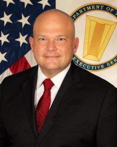
 Mr. Christopher P. Manning, Director of the Command, Power and Integration Directorate (CP&ID)
Title: Power and Energy for the Future U.S. Army
 Dr. Don Tan, NGAS Distinguished Engineer and Power Products Manager, Northrop Grumman Aerospace Systems
Title: Ultra High Power Density Demands 99% Efficiency and 99% Duty Ratio
+ Dr. Babu Chalamala, Manager of the Energy Storage Technology and Systems Department, Sandia National Laboratories
Title: Emerging eT&D Grids: Energy Storage, Electrification, and the Increasing Role of Power Electronics
Abstract: Emerging electronic transmission and distribution (eT&D) grids will evolve rapidly accommodating the changes in generation mix and load profile that are associated with increasing renewable and distributed generation, electrification and bidirectional power flows. For eT&D grids to operate reliably with a high degree of autonomy, there is a greater need for energy storage systems and intelligent power conversion systems with advanced circuit topologies and high speed communication infrastructure. Current challenges for the future eT&D grids include limited scale of energy storage deployments along with low penetration of power electronics in the current grid infrastructure. As we look into a future with 70-80% renewables in the generation mix and higher amounts of dc loads including electric vehicles and appliances, the load profile and operational aspects of the grid will experience changes that are not well forecast. In this presentation, I will review state of eT&D grid development, expected developmental pathways, and projections for eT&D grid in the distant future.
Sandia National Laboratories is a multi-mission laboratory managed and operated by National Technology & Engineering Solutions of Sandia, LLC, a wholly owned subsidiary of Honeywell International Inc., for the U.S. Department of Energy’s National Nuclear Security Administration under contract DE-NA0003525.
Bio: Dr. Babu Chalamala is Head of the Energy Storage Technology and Systems Department and Laboratory Program Manager for Grid Energy Storage at Sandia National Laboratories, Albuquerque, NM. Prior to joining Sandia in 2015, he spent twenty years in industry R&D, mostly recently as a Corporate Fellow at MEMC Electronic Materials/SunEdison where he led R&D and product development in grid scale energy storage. Before that, he was involved in two startup companies for eight years. He spent early part of his research career at Motorola and Texas Instruments where he made contributions to electronic materials and display technologies. He has a B.Tech. in Electronics and Communications Engineering from Sri Venkateswara University and a PhD in Physics from the University of North Texas. An IEEE Fellow, he served on the editorial boards of Proceedings of the IEEE, IEEE Access and IEEE Journal of Display Technology. He currently serves on the as Vice Chair of IEEE PES Energy Storage and Stationary Battery Committee and as a Member of the IEEE Fellow Committee. He has also been active in the Materials Research Society, where he served as a General Chair of the 2006 MRS Fall meeting. He currently serves on the MRS Government Affairs and Award Committees. Author of over 120 papers, several edited volumes, and awarded 10 US patents.
+ Dr. Lauren Boteler, U.S. Army Research Laboratory (ARL), Advanced Power Electronics Group
Title: Co-Design: A Paradigm Shift to Enable Next-Generation Power Modules
Abstract: The Army is moving to a more electrified force for an increasing number of applications including vehicles, renewables, tactical energy networks, communications, and weapons systems. Current power electronics devices are unable to realize their full potential due to the challenges of standard packaging including thermal dissipation, reliability, and parasitic inductance. As technology advances, the electrical, thermal, and reliability needs of these systems must be simultaneously accounted for due to the need for more power in smaller units with no loss in performance. Unfortunately, most research has focused on solving only one technical challenge: a better heat sink, a better circuit design or a more reliable material. When thermal design is treated as a discrete step and not addressed until the end of development, systems become large, overly complex, and inefficient. This presentation will introduce the concept of co-design, a paradigm shift which moves away from the siloed approach to design and transitions into multi-disciplinary design to enable holistic improvement for next generation power electronics. The presentation will cover the current thermal and packaging challenges associated with power modules and will define the three key enabling capabilities to enable future power modules and next-generation cooling solutions: (1) parametric modeling tools, (2) additive manufacturing and (3) transient thermal mitigation.
Bio: Dr. Lauren Boteler leads the thermal and packaging research programs as part of the Advanced Power Electronics group at the U.S. Army Research Laboratory (ARL). She received her PhD degree in mechanical engineering from the University of Maryland. Her work at ARL, beginning in 2005, has included electronics packaging and thermal management solutions for a wide range of Army applications. Her focus is on design tool development and package integrated thermal solutions including 3D chip stacking, power electronics, laser diodes, double side cooling, and phase change materials. More recently, she has initiated a research program in Advanced Power Electronics Packaging and Thermal Management which defined the four main challenges and opportunities of power electronics packaging: co-engineering/co-design, transient thermal mitigation, additive manufacturing, and high-voltage packaging. She is an adjunct professor at Johns Hopkins University and was awarded the 2018 ASME EPPD Woman Engineer of the Year award for her contributions to the electronics packaging community.
+ Dr. Alain Charles, Vice President, Technology Development Center, Infineon Technologies Americas Corp.
Title: Integration of Gallium Nitride in Power Applications: Achievements and Challenges
Abstract: The U.S. Department of Energy has recognize the opportunity to reduce dramatically usage of electricity in homes and businesses through adoption of variable speed motor control. An estimated 535 x 1012 BTU of energy could be saved annually in the US through use of variable speed drive (VSD) in home appliances and an additional 461 x1012 BTU’s when commercial appliances are considered. In total, this is the equivalent of reducing annual release of greenhouse gases due to the usage of 5.5 million short tons of coal.Today VSD are inverterized based on state of the art (SOA) silicon based power solution using either 6 FREDFET power MOSFET or 6 IGBT/FRD pairs together with a gate driver IC capable to drive all 6 switches as a voltage source. The proposed concept is to leverage existing 600V normally off (e-mode) CoolGaNTM switches for use in our VSD “power stages” which feature package integration of 6 GaN HEMT. The reverse recovery performance of CoolGaNTM, provides substantial advantage in term of turn on Loss at full and partial load enabling > 50% reduction in power loss. For successful adoption in motor control, 3 elements of a GaN-based solution are required:
a.) a low cost driver IC which provides current source drive signal as the CoolGaNTM gate is current driven, and protect functions (control slew rate to <5V/ns). The IC must also cost no more than existing low cost voltage source IC’s used with silicon. In this paper, we will describe the proposed solution to realize this IC based on Junction Isolated level shifting technology. b.) A Competitive cost GaN devices. For RDS(ON) values in the 1 ohm range CoolGaNTM die are 5x to 6X times smaller than FREDFET’s so that even with higher wafer cost per area the GaN die cost will be lower than silicon. On top, the lateral nature of the GaN device brings the potential further advantage to integrate monolithically the 6 GaN switches into one die. The paper, will show the challenge to do so, due to the back gating of the high side switch by the low side switch, due to the common silicon substrate, and the proposed remedy to this problem. c.) A low cost surface-mount package solution achieved through the simplification of the 12×12 mm QFN package due to the monolithically integrated GaN switches, which reduces the number of components in the package from 7 (or 13 in case of IGBT) to 2.
Bio: Dr. Charles is a 30 years semiconductor industry veteran. He received his Ph.D. in 1989 from the Institut National des Sciences Appliquées (INSA) de Toulouse (France) for his work on optical lithography for microelectronics. Through his international career, Dr. Charles was involved in most of the key technology changes of the semiconductor industry, like subwavelength pattern printing, to larger wafer (300mm) technology development to power efficiency and introduction of wide bandgap semiconductors. His international career started from driving Optical lithography effort at Motorola Mesa site (AZ, USA) and later ST-Microelectronics factory in Carrollton, (TX, USA). He later joined Motorola-Siemens Joint venture in Dresden pioneering 300mm Silicon manufacturing in Dresden, Germany, and was part of the team that produced the first 64Gbit DRAM on 300mm wafers in 1998. He then managed Fab5 and Fab3 engineering teams at Silicon Foundry Chartered Semiconductor (today Global Foundries) in Singapore. In 2003 is joined International Rectifier power device technology development team, in Newport (Wales, UK), to finally head the silicon technology development team for all discrete power devices from company headquarter in El Segundo, CA, USA. After Infineon acquisition of International Rectifier, he took the worldwide responsibility for the Gallium Nitride technology development initiative within the company.
+ Mr. Christopher P. Manning, Director of the Command, Power and Integration Directorate (CP&ID)
Title: Power and Energy for the Future U.S. Army
Abstract: The U.S. Army recently established the Army Futures Command to develop revolutionary technology for military applications. Intelligent power and energy architecture will be essential as the Army’s needs for mobile power continue to grow. The Army has achieved considerable success in improved fuel consumption by applying the principles of smart grids to battlefield electric power generation. A further level of sophistication must be implemented to such grid design because the number and power ratings of power generators and loads may vary often over time and location. Areas of opportunity for such power and energy technology include advanced power sources, including renewables, generators and batteries, advanced power conditioning devices and more sophisticated thermal management.
Bio: Mr. Christopher P. Manning serves as the Director of the Command, Power and Integration Directorate (CP&ID) in the U.S. Army Combat Capabilities Development Command – C5ISR Center. He is responsible for planning and executing the Army’s science and technology investments in mission command; positioning, navigation and timing; power and energy; and quick-reaction prototyping technology. Mr. Manning entered the Senior Executive Service in 2018. He previously served as the Division Chief of CP&ID’s Prototyping, Integration and Testing Division.
Mr. Manning was commissioned as a Second Lieutenant, Signal Corps, through the Reserve Officer Training Corps (ROTC) at Michigan State University where he graduated from the Honors College with a Bachelor of Science Degree in Electrical Engineering. He later completed his graduate studies at the University of Pennsylvania with a Master’s of Science degree in Engineering.
His first military assignment was Communications Platoon Leader for 4th Battalion, 7th Air Defense Artillery (PATRIOT) at Fort Lewis, Washington. He later served as Executive Officer for D Company, 29th Signal Battalion at Fort Lewis, WA. His other assignments included Assistant S-3 (Systems Integration Branch) and Assistant S-3 (Operations) for 22nd Signal Brigade in Darmstadt, Germany. He commanded the 578th Signal Company for 24 months including a deployment to Iraq in support of Operation Iraqi Freedom. Upon completion of company command, he was assigned to the Army Acquisition Corps. His last military assignment was Assistant Product Manager, Firefinder Radars, at Fort Monmouth, New Jersey.
Mr. Manning accepted an appointment as a Department of the Army Civilian with assignments as Chief Engineer for Product Manager Global Positioning Systems (GPS) and later as Chief, Control Management Systems, in the Software Engineering Directorate of the Communication-Electronics Research, Development, and Engineering Center (CERDEC). He then served as the Deputy Product Manager for GPS from October 2006 through May 2010. From 2010 to 2013, Mr. Manning was chartered as the first Project Director for Communications Security under PEO C3T and charged with staffing, building, and establishing the program office. In 2013, he deployed to Afghanistan in support of Operation Enduring Freedom as the Deputy Director Forward Operations for the Office of the Assistant Secretary of the Army (Acquisition, Logistics and Technology). He also served as the Deputy Chief of Staff for PEO C3T.
His leadership training includes the DAU Senior Service College Fellowship, the Civilian Education System Advanced Course, the Combined Arms and Services Staff School, the Signal Captain’s Career Course (Distinguished Honor Graduate), and the Signal Officer Basic Course (Distinguished Honor Graduate).
Mr. Manning’s military awards and decorations include the Bronze Star Medal, the Meritorious Service Medal with Oak Leaf Cluster, the Army Commendation Medal with Oak Leaf Cluster, the Army Achievement Medal with two Oak Leaf Clusters, the Army Superior Unit Award, the National Defense Service Medal (Second Award), the Armed Forces Expeditionary Medal, the Global War on Terrorism Expeditionary Medal, the Global War on Terrorism Service Medal, and the Overseas Service Ribbon.
His civilian awards include the Superior Civilian Service Award (second award), the Commander’s Award for Civilian Service, the Achievement Medal for Civilian Service, the Global War on Terrorism Medal, and the NATO Medal.
The Signal Corps Regimental Association recognized his contributions with a Bronze Order of Mercury, and U.S. Army Field Artillery Association awarded him the Honorable Order of St. Barbara.
+ Dr. Don Tan, NGAS Distinguished Engineer and Power Products Manager, Northrop Grumman Aerospace Systems
Title: Ultra High Power Density Demands 99% Efficiency and 99% Duty Ratio
Abstract: Recent technology progress demonstrated effective ways of obtaining 99% power efficiency. The near adiabatic power conversion technology, for instance, needs no dedicated thermal management. Yet ultra-high power density has eluded many designs. The most recent technology trend in power conversion, particularly for dc-dc, suggests a significant increase in power density is within reach. Ultra-high power density in commercial products demands a 99% efficiency and a virtual full duty ratio (say, 99%). The path forward requires a systematic approach in leveraging distributed low-profile packaging, minimum inductive storage, capacitive energy transfer, partial power processing, integrated WBG devices, modularity, and scalability. It is anticipated that the power electronics industry will achieve an-order-of-magnitude improvement in achievable power density within the coming years.
Bio: Dr. Tan is NGAS Distinguished Engineer and Power Products Manager. He earned his Ph.D. degree from Caltech and is IEEE Fellow (since 2007). Well-recognized as an authority in near adiabatic power conversion and energy systems, he has pioneered many breakthrough innovations with high-impact industry firsts and record performances. His technologies have attracted significant customer funding and led to four product lines for the company and with hundreds of designs and thousands of delivered flight hardware that “significantly enhancing national security.” He has given more than 50 keynotes and invited talks. He serves frequently on national and international funding, review, award, and prestigious position selection committees.

Join Our Conversation